
A Suprising Discovery Inside The Steam Deck's APU
Following an excellent Youtube video from HighYield recently, we have learnt two things about the design of the APU used in the Steam Deck LCD version:
- The Steam Deck APU (codenamed Van Gogh) has unused parts with a lot more cores. And it is very likely that the exact same APU was also used for the Magic Leap 2 AR glasses, which makes use of such cores.
- The Steam Deck APU used in the OLED version may be the first chipset entirely made for the Steam Deck platform, with a smaller footprint not just thanks to the 6nm lithography, but because the unused cores were removed.
Now that you know what we are going to look at, let’s see the whole story in pictures.
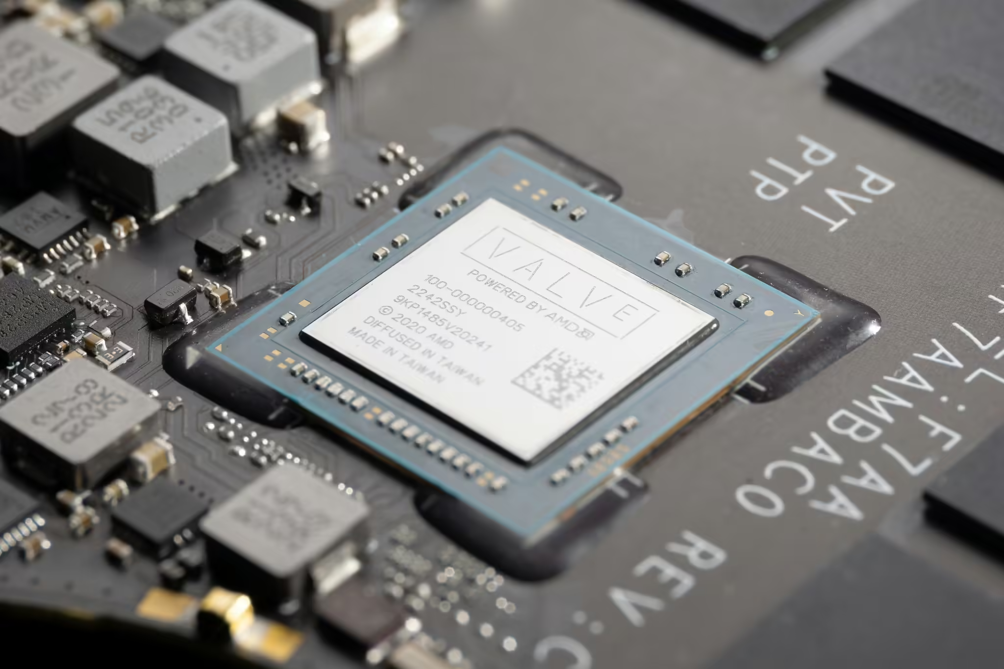
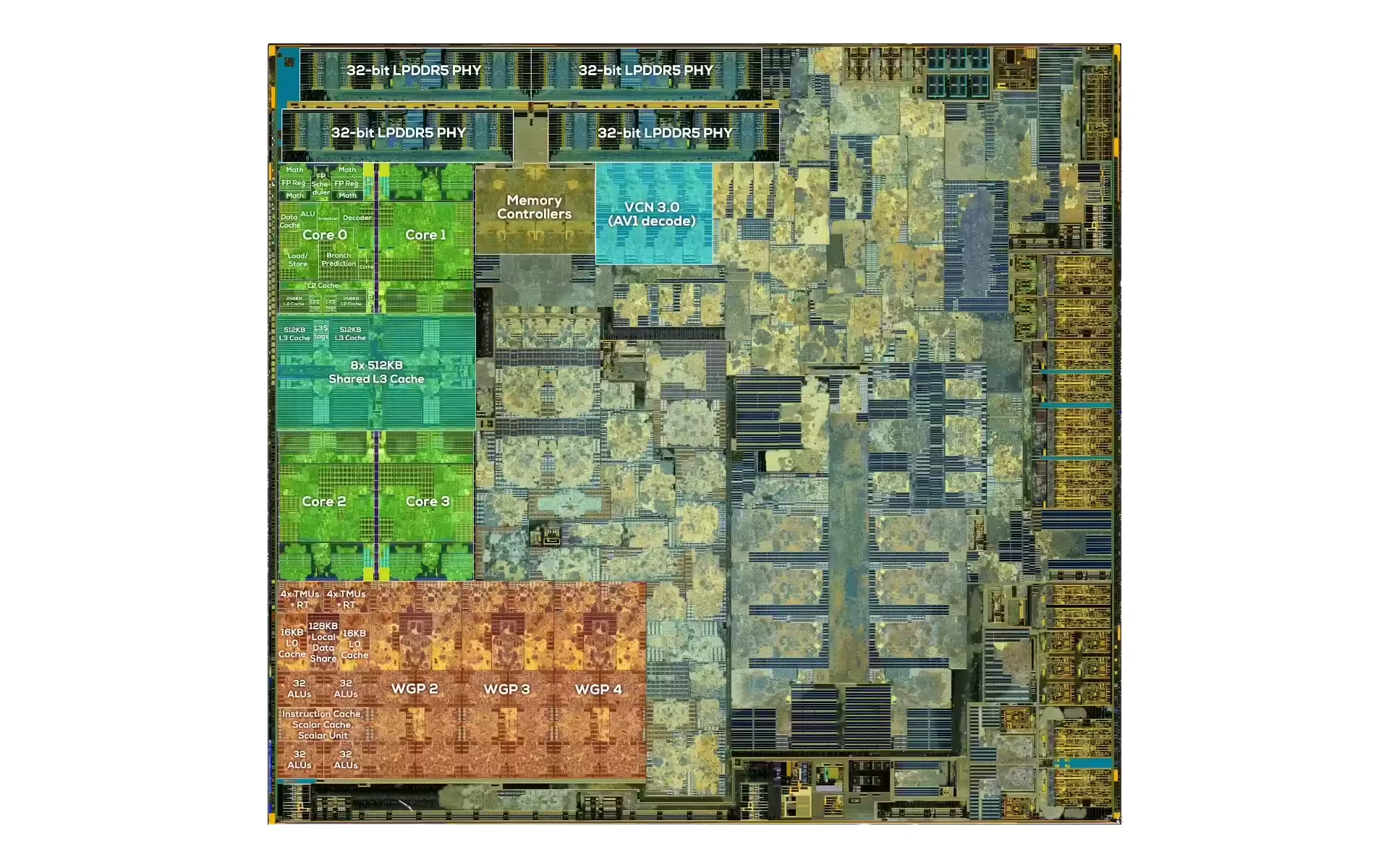
The Steam Deck APU
The Van Gogh APU combines a high-performance CPU with AMD RDNA 2 architecture-based GPU cores, delivering good graphics and processing capabilities with a focus on energy efficiency. It makes it a good candidate for handheld devices like the Steam Deck.
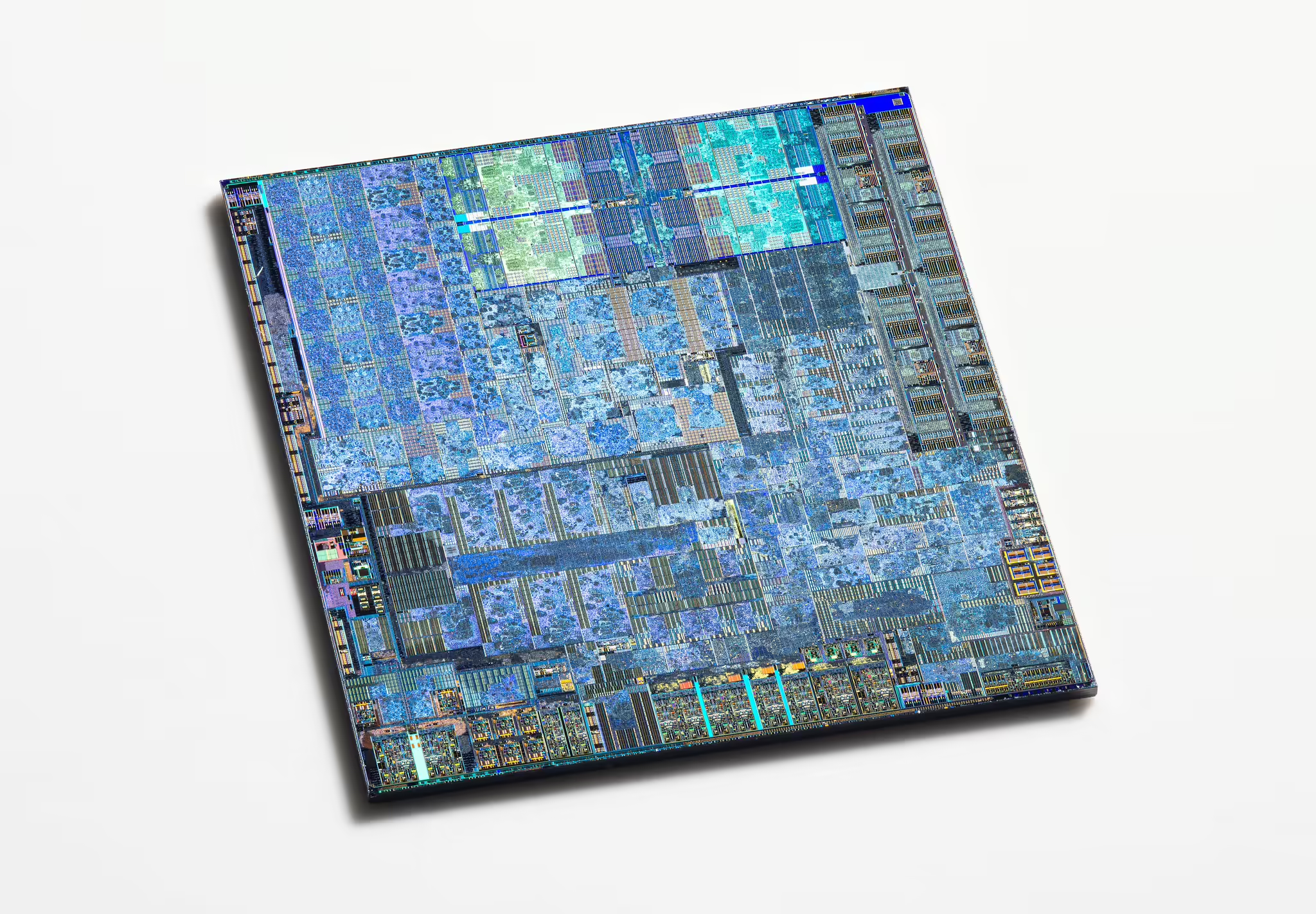
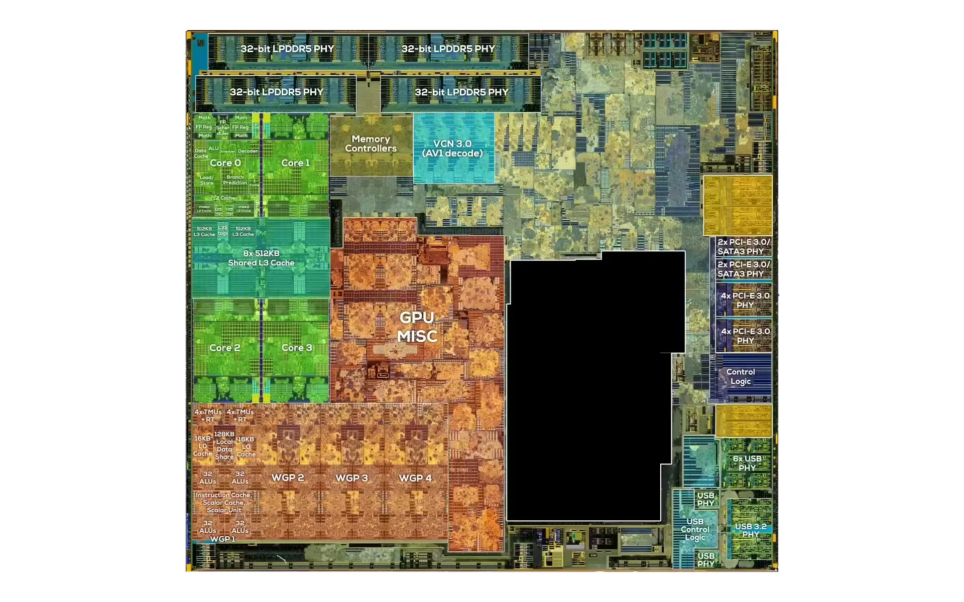
Thanks to the detailed pictures of Fritzchens Fritz we now have a clear idea of how the Van Gogh APU is split, in details.
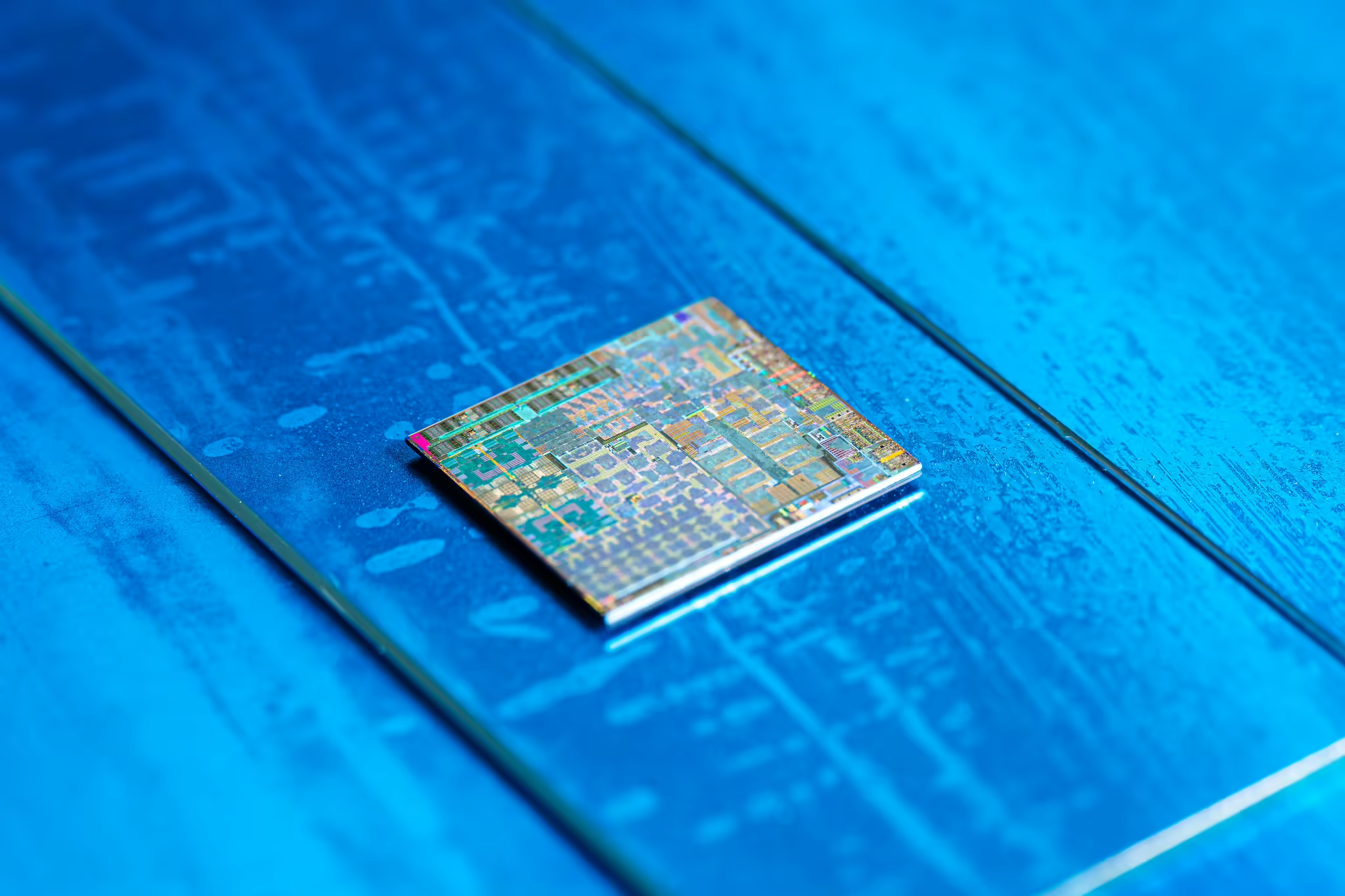
Another angle:
The Memory and CPU Cores
As expected we can see the memory controllers just next to the CPU cores. There are 4 CPU cores, and they all share the L3-level cache which is just built in between the CPU cores.
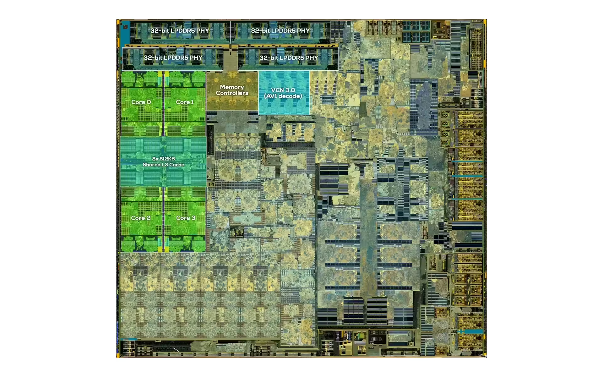
So far, nothing surprising, and you can see how small the CPU cores actually are in modern processors.
The GPU
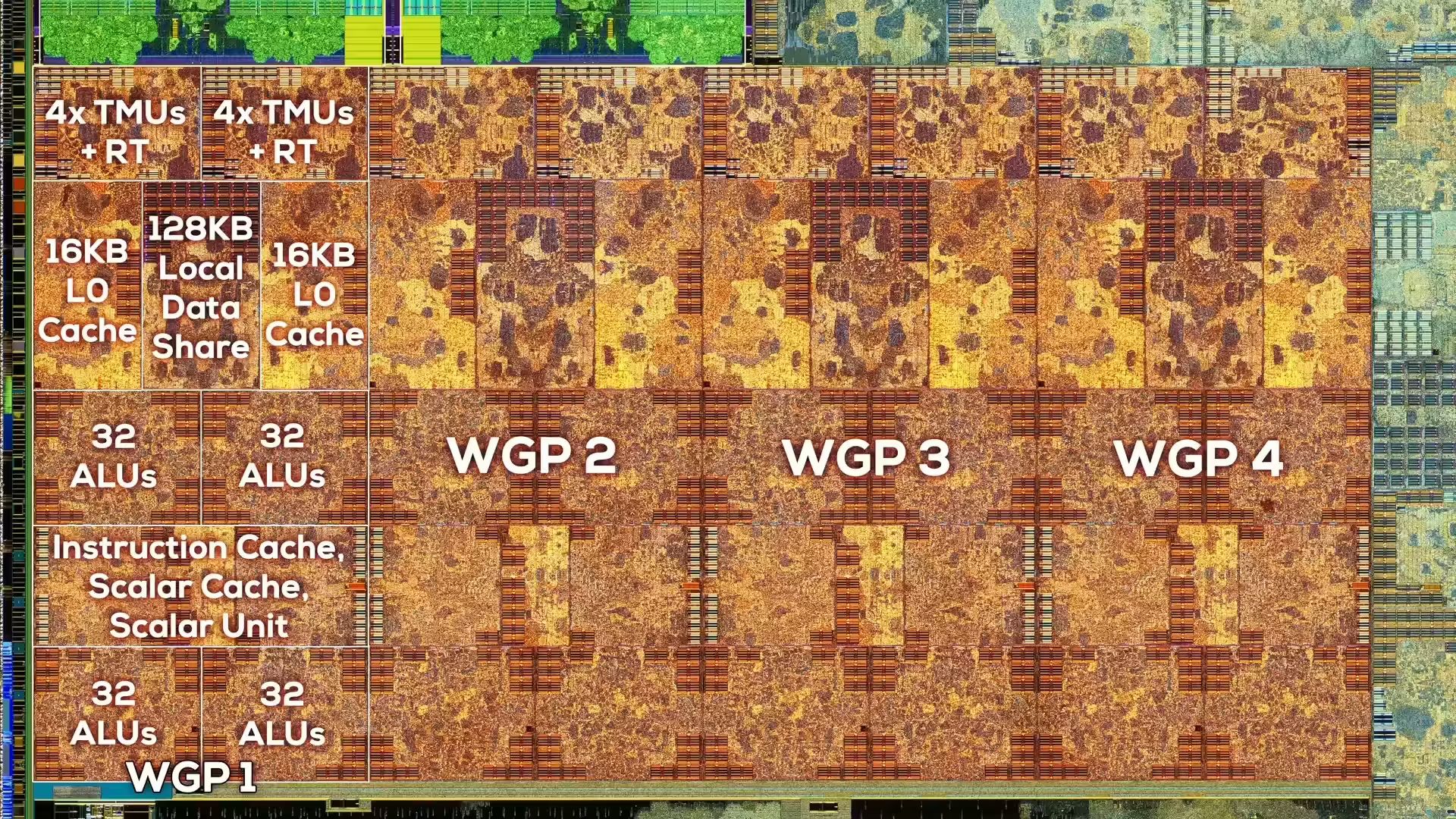
The RDNA 2 GPU Cores
The GPU cores are separate in 4 WGP (workgroup processors).
They feature several sub-parts:
- Several layers of cache
- 4 units of 32 ALUs (Arithmetic Logic Units) for vector processing
- 2 units of 4 TMUs (Texture Mapping Units) together with Ray-Tracing units.
While it may come as a surprise, the Steam Deck can actually do some Ray-Tracing while it is fairly weak in that regard. It has however been implemented to support a few games such as Doom Eternal.
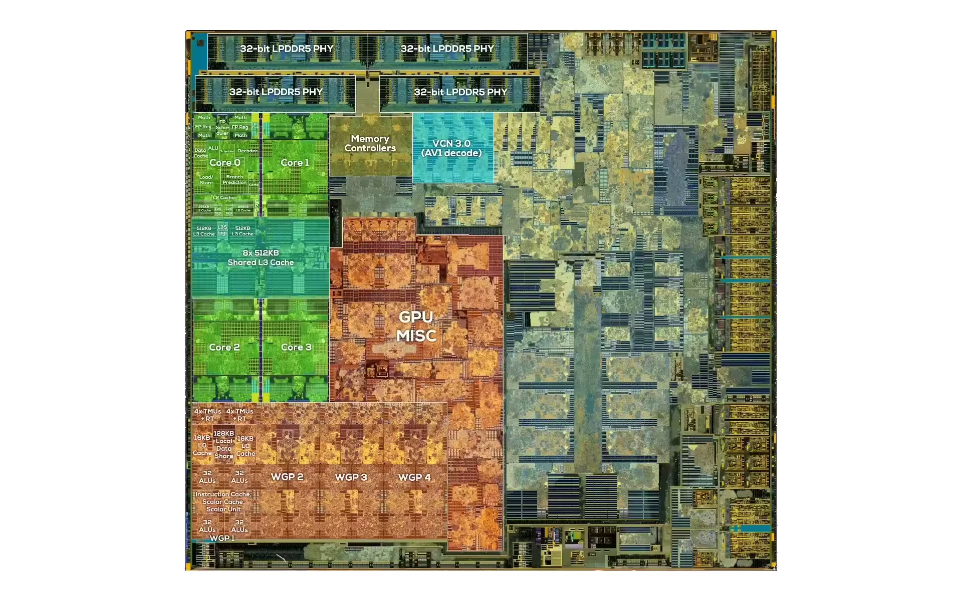
There is some additional GPU Misc parts that probably handle many other things (memory transfer, encoding, your guess is as good as mine) that space a significant amount of die space.
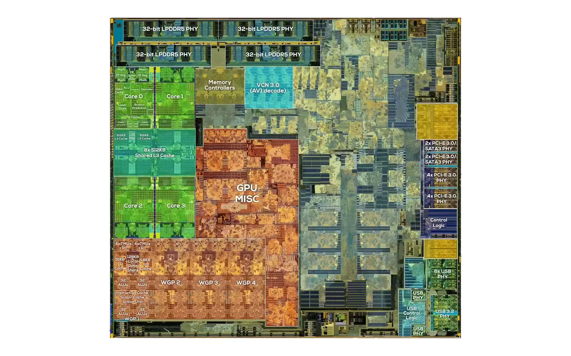
Of course, there are also additional connectors on the right side of the chip for various I/O ports, like SATA, USB and more.
But it still does not explain what we have here at the middle right side of the chip.
The Mysterious parts
There’s a part that represents almost 15% of the surface that is completely undocumented.
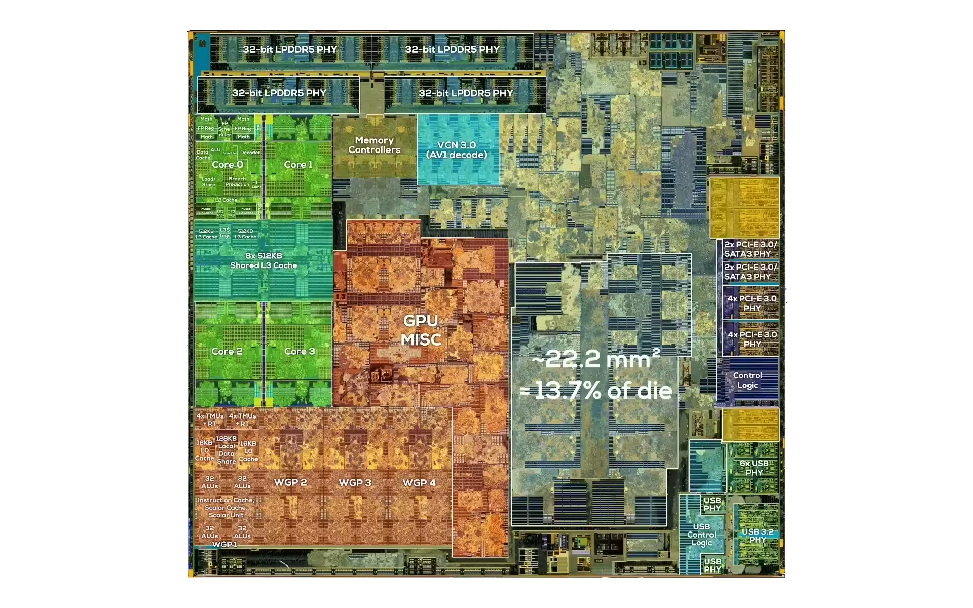
It contains additional cores, and the heteregoneous kind. 14 additional cores to be exact.
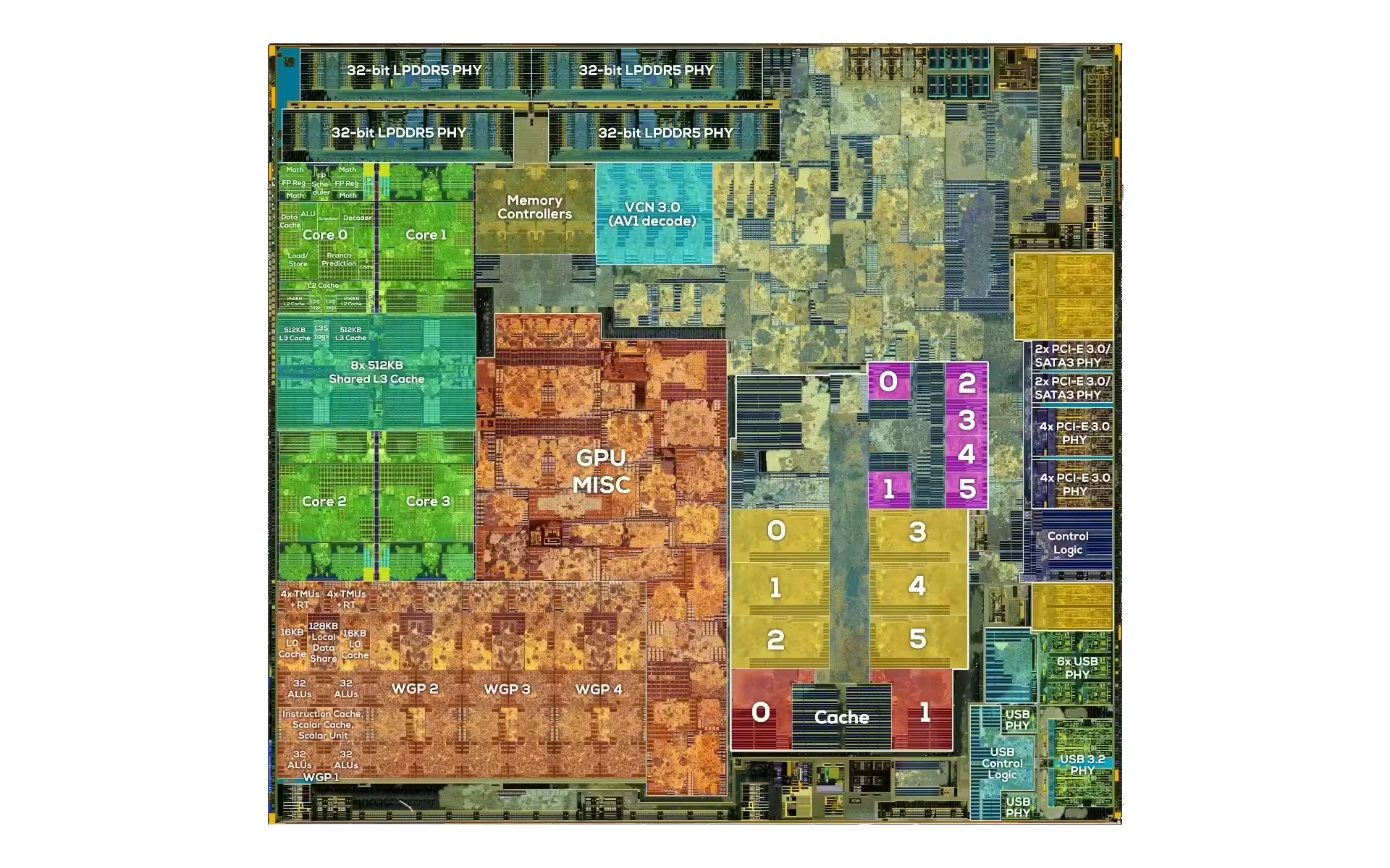
Turns out, this part is additional GPU cores, and it seems to be completely consistent with the description of the chipset used in the Compute Pack for the Magic Leap 2 AR glasses.
You can see the specs below:
| Category | Magic Leap 2 | Steam Deck |
|---|---|---|
| GPU | AMD RDNA 2 2 RB+ (Render Backends) Max Gfx frequency capped at 1.1 GHz. |
AMD RDNA 2 Max Gfx frequency 1.6GHz |
| CPU | AMD 7nm Quad—core Zen 2 x86-64 core (8 threads) 14 core computer vision processing engine (CVIP) Max CPU frequency 2.4 GHz Cache sizes: 512kB L2 per core and 4MB total L3 cache. |
AMD 7nm Quad—core Zen 2 x86-64 core (8 threads) CPU frequency 2.4-3.5GHz Cache sizes: 512kB L2 per core and 4MB total L3 cache. |
As you can see the 14 cores seem to be clearly mentioned in the specs sheet of the Magic Leap 2, and are used for image processing. While some of the frequencies used internally between the two chipsets are different (the Steam Deck uses higher frequencies) it’s plausible that they share the exact same architecture, and that these 14 additional cores visible on the Steam Deck LCD APU were actually made for the Magic Leap 2 in the first place.
Differences between the LCD and OLED Steam Deck APU
The video continues by explaining that the difference in surface area between the Steam Deck LCD APU and the new version as found on the newer Steam Deck OLED APU are fairly large: the new APU is much smaller in size.
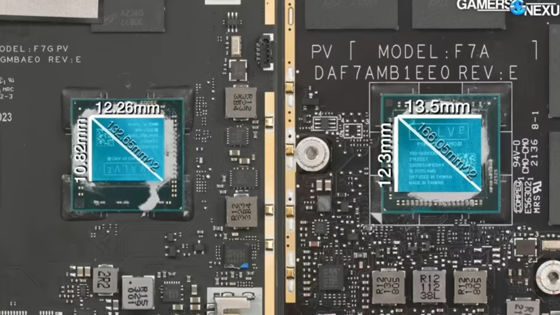
This is however not consistent with the kind of progress we expect from the TSMC process when moving from 7nm to 6nm, as most of the improvements in density do not broadly apply across the board but only for specific logic circuitry.
So the hypothesis, that remains to be proven, is that the Steam Deck OLED APU is actually made specifically for the Steam Deck this time, and does away with the 14 cores used by the Magic Leap 2 since they are not needed on the Steam Deck.
This seems to match the huge surface reduction observed in the chip area on the new board. At that point in time, Valve would have been able to predict how many units they could expect to sell based on previous shipments, and order fully customized chips for their new Steam Deck revision.
This also sounds like Valve will have opportunities down the road to further customize what goes in their Steam Deck 2 platform, vs using more generic chip designs from AMD that may not fit the lower power envelope targeted by the Steam Deck.
Closing Words
Since this article made it to HN, there’s one comment from HN user exmadscientist that I would like to add at the end, to give a potential explanation to what may have happened at the time the Steam Deck was in the works:
My guess is that Magic Leap, a company infamous for spending profligately, paid for the NRE on this design, and then didn’t buy very many of them or pay for exclusivity on it (or let any exclusivity go). AMD is notorious for shopping around designs they’ve already got ready to ship (probably related to sibling comment’s observations about the console graphics market), and Valve runs lean despite not having to, and so this story adds up quite nicely. There may or may not have been some inventory lying around, but the NRE is usually the real story on these things. (It’s also possible that the custom Magic Leap sections of this chip have terrible yield – actually that wouldn’t surprise me at all – and so these were great candidates for die harvest. Which of course is also the sort of thing AMD loves to sell.)
Another comment from HN user danpalmer echoes the same sentiment:
Sounds like Magic Leap “overspent” on a custom chip design and fab, like they overspent on everything else, and ended up with a fraction of the sales they expected. And then Valve “underspent” (although perhaps more of an MVP) by taking an existing good-enough chip, perhaps able to get very good yield out of fab (at a time when fabs were costing a fortune), and found yet another corner to cut on a device that is overall pretty low build quality, to hit an aggressive price point. I love my Steam Deck, and I loved the low price, but the build quality is “good enough” at best. Valve have reversed course with the new generation, having a custom chip now that they’ve proved out the demand, and I expect the device will improve across the board as they take advantage of higher volumes, and perhaps an ability to price a little higher too. I wouldn’t be surprised if Magic Leap also reverse course (or already have done? are they still around?) by moving to much cheaper off the shelf or pre-existing hardware.
There are many other great comments in that thread, so I recommend you check them as well.